Posted on Friday, June 19 2009 @ 2:56 CEST by Thomas De Maesschalck
Toshiba researchers have made a breakthrough which could have significance for future development of chips at 16nm processes.
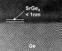
Toshiba said it has overcome the challenge of fabricating a thin gate stack while maintaining high hole mobility, by inserting SrGex, a compound of strontium (Sr) and germanium, as an interlayer between the high-k insulating layer and the germanium channel.
The technology realises peak hole mobility of 481cm sq./Volt-second.
Toshiba will continue to develop the technology as an option toward implementation of Ge-MISFET to 16nm chips and beyond.
More info
at Electronics Weekly.