Posted on Sunday, March 21 2010 @ 14:10 CET by Thomas De Maesschalck
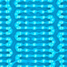
Scientists at MIT are exploring molecules that arrange themselves into predictable patterns on silicon chips, a technology that could lead to computer chips with much smaller circuit elements. More details
at MITnews.
Currently, chips are built up, layer by layer, through a process called photolithography. A layer of silicon, metal, or some other material is deposited on a chip and coated with a light-sensitive material, called a photoresist. Light shining through a kind of stencil — a “mask” — projects a detailed pattern onto the photoresist, which hardens where it’s exposed. The unhardened photoresist is washed away, and chemicals etch away the bare material underneath.
The problem is that chip features are now significantly smaller than the wavelength of the light used to make them. Manufacturers have developed various tricks to get light to produce patterns smaller than its own wavelength, but they won’t work at smaller scales..