Posted on Monday, February 28 2011 @ 18:11 CET by Thomas De Maesschalck
The Register has written a piece about AMD's new Bulldozer core, you can check it out
over here. The article is based on the information revealed at last week's IEEE International Solid-State Circuits Conference in San Francisco.
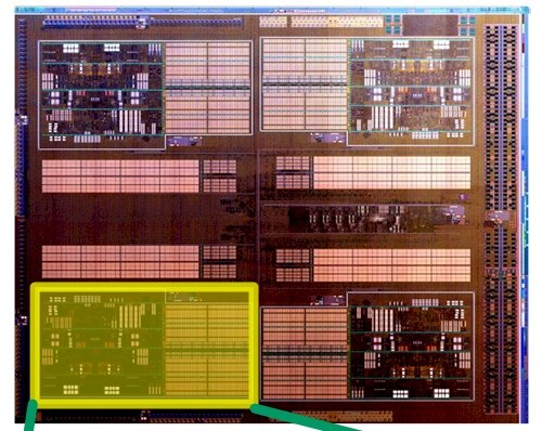
Up until this time, AMD has only been showing an abstracted block diagram of the Bulldozer module. As El Reg has previously reported, the Bulldozer core is implemented in GlobalFoundries' 32nm, 11-metal layer, high-k metal gate, silicon-on-insulator wafer-baking processes. The idea behind the core module is to have some components shared across two cores, but to give each core its own thread (with no simultaneous multithreading) to have two strong cores. Each core – which means an integer unit and a floating point unit – in the Bulldozer module has its own integer unit scheduler and L1 data caches, but the cores share fetch and decode units as well as a floating point scheduler and L2 cache memory.