Posted on Tuesday, July 10 2012 @ 19:29 CEST by Thomas De Maesschalck
SEMI senior analyst Christian Dieseldorff
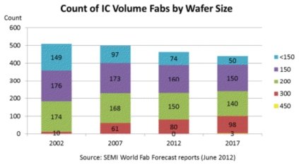
the first 450mm wafer fabs are projected to commence operation in 2017. Widespread adoption is expected by 2018 at the earliest, but more likely in 2019 or 2020.
In a presentation at the Semicon West tradeshow here Monday (July 9), Dieseldorff predicted that three 450-mm fabs would commence operation in 2017. By that time, the total number of IC production fabs will have declined to 441, down from 464 this year, according to Dieseldorf.
Several industry development projects are now focused on developing tools for 450-mm wafers, which leading edge chip makers want to transition to in order to increase the number of die per wafer, and thus profitability. Among these projects is the Global 450 Consortium, a $4.8 billion collaboration housed at the Albany NanoTech complex in New York and backed by semiconductor industry heavyweights Intel Corp., IBM Corp., Globalfoundries Inc., Samsung Electronics Co. Ltd. and Taiwan Semiconductor Manufacturing Co. Ltd. (TSMC).