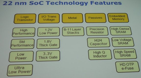
The new process differs from Ivy Bridge's 22nm process by offering lower leakage logic transistors, higher voltage I/O transistors, denser upper layer interconnects, and a set of precision resistors, capacitors and inductors.
“It’s not one set of features, but a menu of feature options—transistors, I/O, interconnects, passive elements and embedded memory,” Bohr said. “The [SoC] transistors go down to much lower leakage levels, but give up some performance,” he said.
The process has significantly better analog characteristics than Intel’s current 32-nm planar process. Designs make heavy use of 80-nm pitch features in lower metal layers, because they are the smallest features Intel can make at 22 nm without needing double patterning, he added.

Source: EE Times