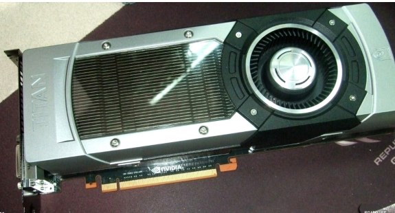
According to the leaked specifications, this card has two 28nm GK110-based GPUs, with 2688 CUDA cores, 224 TMUs, 48 ROPs, a 384-bit memory bus, 837MHz core, 878MHz GPU Boost, 6GB GDDR5 memory clocked at 6008MHz and a 250W TDP.
The GeForce GTX Titan PCB reveals that NVIDIA isn't using a full-coverage IHS on the GK110 ASIC, rather just a support brace. This allows enthusiasts to apply TIM directly on the chip's die. The GPU is wired to a total of twenty four 2 Gbit GDDR5 memory chips, twelve on each side of the PCB. The card's VRM appears to consist of a 6+2 phase design which uses tantalum capacitors, slimline chokes, and driver-MOSFETs. The PCB features a 4-pin PWM fan power output, and a 2-pin LED logo power output that's software controllable.

