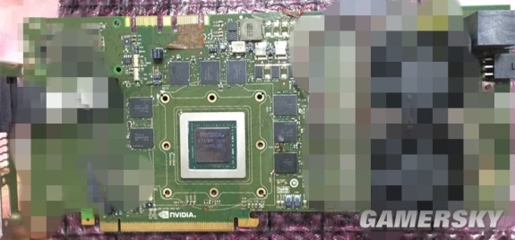
The card looks like an engineering sample and based on what you can see it features 8GB GDDR5 memory, the memory chips are the SK Hynix' H5GQ4H24MFR, which offer a frequency of 7000MHz. VideoCardz thinks the GTX 880 will launch with 4GB and will later be accompanied by 8GB versions.
The other interesting bit, is that the sample is equipped with 3 power connectors (6+6+8pin). It is nothing we were expecting from power efficient Maxwell architecture, but it could be just a feature for engineering sample. Either way, the absolute maximum power draw should not exceed 375W (75+75+75+150).
We can still see SLI fingers on the top, which indicates that NVIDIA has not decided to follow AMD’s path with XDMA CrossFire. The oldschool SLI connectors might still be required.
I’m not exactly sure what is hidden behind pixelated power section. All we can see are two rather large components group. Are there any ARM cores hidden there?