AMD reveals the Vega architecture, Vega chip gets pictured

Posted on Thursday, January 05 2017 @ 16:12 CET by Thomas De Maesschalck
As expected, AMD's Vega slideware has arrived. The company shared information about the architectural improvements it made but the juicy details like card details, performance, power consumption and pricing were not revealed. The company is also still clinging to a "first half of 2017" launch date so I think it's safe to assume we won't see any cards in decent volume until April at the earliest, and possibly even later than that.

For an in-depth look at the new architecture I suggest this article from The Tech Report. Among other things, it describes the new memory architecture, the new geometry pipeline with higher throughput per clock and improved load balancing, the new compute unit design, and the redesigned pixel engine. Another interesting new feature of Vega is the implementation of Primitive Shader, this is run on a more programmable geometry pipeline stage and has the goal to handle geometry data more effectively.

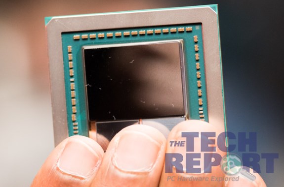
The site's reporter was also able to hold a Vega chip in his hands and took a picture of the package, which shows off the Vega GPU and two HBM2 stacks. VideoCardz took out the digital ruler and estimates the Vega chip has a die size of 520-540mm².

AMD Vega HBM2 first photo of chip

Additionally, there are a bunch of new Vega videos on YouTube. Here's a brief clip of Vega running Doom on Ultra settings at 4K:


A brief rundown of the new architecture:


And how Vega will benefit gamers:


About the Author

Thomas De Maesschalck

Thomas has been messing with computer since early childhood and firmly believes the Internet is the best thing since sliced bread. Enjoys playing with new tech, is fascinated by science, and passionate about financial markets. When not behind a computer, he can be found with running shoes on or lifting heavy weights in the weight room.


Loading Comments