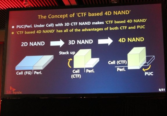
SK Hynix's new 4D NAND uses a charge trap design, just like the flash produced by Samsung and WD/Toshiba. SK Hynix has used Charge Trap Flash (CTF) designs for several years, so it isn't new, and currently Micron and Intel are the only two flash-fabbers using floating gate technology. Intel and Micron plan to diverge on their flash development efforts after their next-gen flash comes to market, after which Micron will use its own 'Replacement Gate' technology, which is simply a re-branded Charge Trap Flash design. In other words, Intel will soon be the only flash producer using floating gate technology.In its presentation, SK Hynix revealed it sees a path for 4D NAND up to more than 500 layers. At present, SK Hynix's most advanced flash memory uses 96 layers. A timeline wasn't provided, flash with that many layers is still years away. The first 4D NAND from SK Hynix will sample in Q4 2018, it will be a 96-layer TLC chip with a capacity of 512Gb. A QLC-based version is expected in the second half of 2019.
SK Hynix promises 4D NAND will offer a 30 percent reduction in chip size versus its current 3D NAND, a 30 percent increase in write performance, a 25 percent increase in read performance, and a 150 percent jump in bandwidth/power.