Samsung 3nm MCBFET transistor technology details hit the web

Posted on Tuesday, April 14 2020 @ 17:12 CEST by Thomas De Maesschalck
Samsung logo
Information about Samsung's future process technology hit the web. TechPowerUp reports about Multi Bridge Channel FET (MCBFET), a technology that will be used by Samsung's 3nm Gate-All-Around FET (GAAFET) transistors.

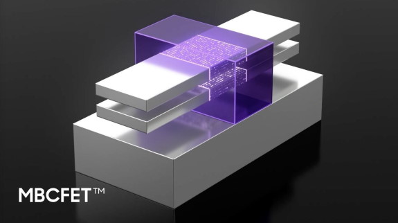
Getting right in to the meat, MCBFET promises 50 percent lower power consumption and 30 percent more performance, as well as a 45 percent reduction in size. The comparison base is an unspecified 7nm node.
The technology allows the stacking of transistors on top of each other, which makes it use inherently less space compared to regular FinFET. Being that MCBFET GAA transistors make its transistor width flexible, it means that the overall stacked transistor can be as wide as a designer needs it to be, adjusting for any scenario like low-power or high-performance.
Based on current plans, Samsung's 3nm process will be used for mass production in 2022.

TSMC logo


About the Author

Thomas De Maesschalck

Thomas has been messing with computer since early childhood and firmly believes the Internet is the best thing since sliced bread. Enjoys playing with new tech, is fascinated by science, and passionate about financial markets. When not behind a computer, he can be found with running shoes on or lifting heavy weights in the weight room.


Loading Comments